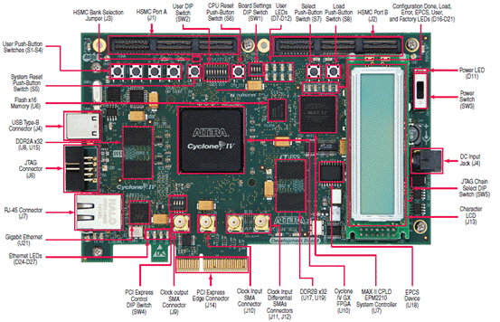
图2.Cyclone IV GX FPGA开发套件外形图和主要元件分布图
The board features the following major component blocks:
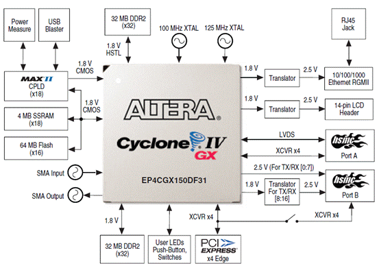
■ Cyclone IV GX EP4CGX150DF31 FPGA in the 896-pin FineLine BGA (FBGA)package
■ 1.2-V core power
■ MAX? II EPM2210GF256 CPLD in the 256-pin FBGA package
■ 1.8-V core power
■ FPGA configuration circuitry
■ MAX II CPLD EPM2210 System Controller and flash fast passive parallel (FPP) configuration
■ Active serial configuration
■ On-board USB-BlasterTM for use with the Quartus? II Programmer
■ JTAG header for external USB-Blaster with the Quartus II Programmer
■ On-Board ports
■ Embedded USB-Blaster
■ One gigabit Ethernet port
■ Communication ports
■ PCI Express (PCIe) edge connector
■ 10/100/1000BASE-T Ethernet PHY with RJ-45 connector
■ Two High-Speed Mezzanine Card (HSMC) interfaces
■ On-Board memory
■ 4-MB (x16) Synchronous Static Random Access Memory (SSRAM)
■ Two 32-MB (x32) DDR2 SDRAM
■ 64-MB flash
■ On-Board clocking circuitry
■ 50.000-MHz oscillator
■ 125.000-MHz oscillator
■ SMA clock input
■ SMA clock output
■ Programmable oscillator (default: 100.000-MHz)
■ General user I/O
■ LEDs and display
■ Eight FPGA user LEDs
■ One configuration done LED
■ One error LED
■ Five Ethernet status LEDs
■ One USB status LED
■ One power status LED
■ Five configuration LEDs
■ A two-line 16-character LCD display
■ Push-Button switches
■ One CPU reset push-button switch
■ One MAX II configuration reset push-button switch
■ One program-load push-button switch—configure the FPGA from flash memory
■ One program-select push-button switch—select image to load from flash memory or serial configuration (EPCS) device
■ Four general user push-button switches
■ DIP switches
■ Board settings DIP switch
■ JTAG chain select DIP switch
■ PCIe control DIP switch
■ Configuration settings DIP switch
■ User DIP switch
■ Power supply
■ 16-V DC input
■ 2.5-mm barrel jack for DC power input
■ On/Off slide power switch
■ On-Board power measurement circuitry
■ 20-W per HSMC interface
■ Mechanical
■ PCIe small form factor board
■ Bench-top operation