微电子技术发展到今天,已提供了几千至几千万个标准门的芯片。特别是在系统可编程技术,可有条件地在一个芯片上设计制作一个数字系统,即系统芯片(System on Chip,SoC)。国内市场上常见的Altera公司、Xilinx公司、Lattice公司的FPGA和CPLD芯片,一般都能满足设计SoC的需要,并且都提供了EDA软件开发工具。而且在现有的软件开发工具中,有电路图、状态图、真值表和硬件描述语言等输入方式。但设计片上并行控制器,难以用电路图或逻辑方程输入方式实现;如果用状态图或真值表输入方式,随着问题复杂程度的增加,系统的状态将发生组合爆炸,这是十分棘手的问题。而且有限状态机(FSM)虽已被广泛运用到数字逻辑控制系统,也只是因为它给出了系统化的硬件实现方法和具体的实现模型(如Moore自动机和Mealy自动机),用FSM实现并行控制器也十分困难。因为FSM必须于设计前划分控制器,所以常常会导致非最优的门级实现,且使设计中并发的数量受到使用FSM数量的限制,同时FSM间相互依赖,使得设计难于验证且易产生并行同步错误(如死锁、丢失数据的完整性)。上述这些缺点只有设计遍历整个状态空间时才能验证,因而可能被漏检[3]。若用硬件描述语言输入,遇到的困难是模型和验证。
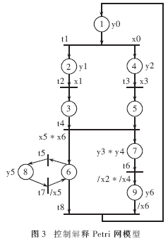
t1<=not p2 and not p4 and x0 and p1;
t2<=not p3 and x1 and p2;
t3<=not p5 and x3 and p4;
t4<=not p6 and not p7 and p3 and p5;
t5<=not p8 and x5 and x6 and p6;
t6<=not p9 and not x2 and not x4 and p7;
t7<=not p6 and not x5 and p8;
t8<=not p1 and not x6 and p6 and p9;
np1<=t8 or (p1 and not t1);
np2<=t1 or (p2 and not t2);
np3<=t2 or (p3 and not t4);
np4<=t1 or (p4 and not t3);
np5<=t3 or (p5 and not t4);
np6<=t4 or t7 or(p6 and not t5 and not t8);
np7<=t4 or (p7 and not t6);
np8<=t5 or (p8 and not t7);
np9<=t6 or (p9 and not t8);