The Spartan-3E family of Field-Programmable Gate Arrays (FPGAs) is specifically designed to meet the needs of high volume, cost-sensitive consumer electronic applications.
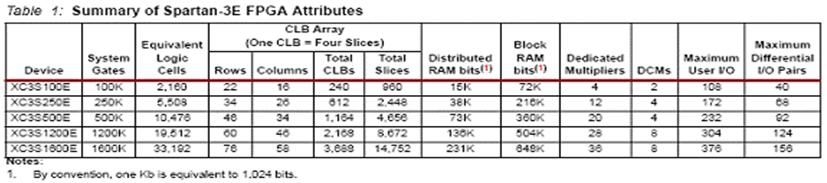
The five-member family offers densities ranging from 100,000 to 1.6 million system gates.The Spartan-3E family builds on the success of the earlier Spartan-3 family by increasing the amount of logic per I/O, significantly reducing the cost per logic cell. New features improve system performance and reduce the cost of configuration.
These Spartan-3E enhancements, combined with advanced 90 nm process technology, deliver more functionality and bandwidth per dollar than was previously possible, setting new standards in the programmable logic industry.
Because of their exceptionally low cost, Spartan-3E FPGAs are ideally suited to a wide range of consumer electronics applications, including broadband access, home networking, display/projection, and digital television equipment.
The Spartan-3E family is a superior alternative to mask programmed ASICs. FPGAs avoid the high initial cost, the lengthy development cycles, and the inherent inflexibility of
conventional ASICs. Also, FPGA programmability permits design upgrades in the field with no hardware replacement necessary, an impossibility with ASICs. Spartan-3E FPGA系列主要特性:
Very low cost, high-performance logic solution for high-volume, consumer-oriented applications
Proven advanced 90-nanometer process technology
Multi-voltage, multi-standard SelectIO interface pins
- Up to 376 I/O pins or 156 differential signal pairs
- LVCMOS, LVTTL, HSTL, and SSTL single-ended signal standards
- 3.3V, 2.5V, 1.8V, 1.5V, and 1.2V signaling
- 622+ Mb/s data transfer rate per I/O
- True LVDS, RSDS, mini-LVDS, differential HSTL/SSTL differential I/O
- Enhanced Double Data Rate (DDR) support
- DDR SDRAM support up to 333 Mb/s
Abundant, flexible logic resources
- Densities up to 33,192 logic cells, including optional shift register or distributed RAM support
- Efficient wide multiplexers, wide logic
- Fast look-ahead carry logic
- Enhanced 18 x 18 multipliers with optional pipeline
- IEEE 1149.1/1532 JTAG programming/debug port
Hierarchical SelectRAM memory architecture
- Up to 648 Kbits of fast block RAM
- Up to 231 Kbits of efficient distributed RAM
Up to eight Digital Clock Managers (DCMs)
- Clock skew elimination (delay locked loop)
- Frequency synthesis, multiplication, division
- High-resolution phase shifting
- Wide frequency range (5 MHz to over 300 MHz)
Eight global clocks plus eight additional clocks per each half of device, plus abundant low-skew routing
Configuration interface to industry-standard PROMs
- Low-cost, space-saving SPI serial Flash PROM
- x8 or x8/x16 parallel NOR Flash PROM
- Low-cost Xilinx Platform Flash with JTAG
Complete Xilinx ISE and WebPACK development system support
MicroBlaze and PicoBlaze embedded processor cores
Fully compliant 32-/64-bit 33 MHz PCI support (66 MHz in some devices)
Low-cost QFP and BGA packaging options
- Common footprints support easy density migration
- Pb-free packaging options
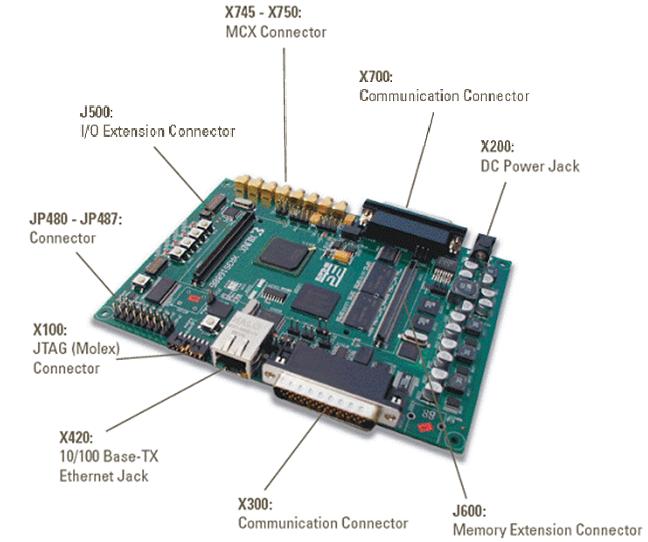
The Automotive ECU Development Kit (HW-XA3S1600E-UNI-G) is a configurable and extensible platform suited for a wide range of automotive applications right out of the box.
With its small form factor, it can be easily placed in standard metal housing. The board was designed to be powered by a 12-volt power supply for in-vehicle prototype use. Powered by a completely field-configurable Spartan-3E FPGA platform, this kit:
Combines programmable logic for custom driven IP applications with the Xilinx MicroBlaze 32-bit microprocessor core.
Features robust memory subsystem containing on-board Flash and SRAM memory.
Supports standard Automotive and System-on-chip peripherals including all necessary physical layers on board the ECU, such as JTAG, 10/100 Ethernet, USB 2.0, 12-bit ADC, High and Low Speed CAN, FlexRay, LIN, K-Line, UART, SPI and over 150 user programmable I/Os.
ECU 开发套件包括:
XA1600E development board with the XC3S1600EFG484 device
Power supply with universal adaptor
Programming cable
Custom serial cable
QuickStart guide
EDK and ISE evaluation tools
Resource CD with reference designs for easy evaluation
ECU 开发套件主要特性:
Xilinx device: XC3S1600EFG484 FPGA
Complete out-of-the box development system
On-board hardware interfaces such as CAN 2.0C, Ethernet 10/100, USB 2.0, SPI, and SCI
Support for pre-verified Xilinx and Partner IP for High and Low Speed CAN, FlexRay and MOST network interfaces.
Daughter card is required for MOST interface.
ECU 开发套件目标应用:
Automotive subsystems
In-vehicle networking systems
Infotainment
Driver assistance and information systems
The XA1600E provides designers with a configurable ECU right out of the box suitable for a wide range of Automotive and Industrial applications.
Please review the following reference manual thoroughly to receive the most of your new purchase.
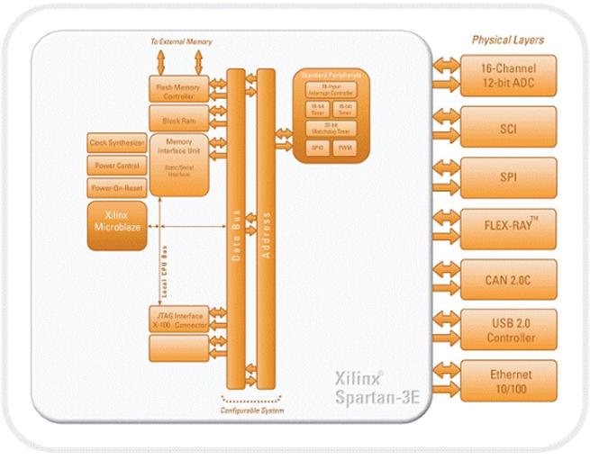
The XA1600E is a complete 32-bit Field Configurable ECU platform, combining the highly popular Xilinx MicroBlaze processor core with standard System-on-Chip peripherals and over 150 user programmable I/O’s. It is contained within a Xilinx Spartan-3A FPGA with programmable logic for custom driven IP applications, a robust memory subsystem, and a full suite of Automotive and Industrial peripherals. The XA1600E enables programmable System-on-Chip applications and expands traditional development platforms by including necessary physical layers onboard the ECU. The XA1600E supports physical layers for 10/100 Ethernet, JTAG, USB 2.0, 12-bit ADC, High and Low Speed CAN, FlexRay, LIN, K-Line, UART, and SPI along with on-board Flash and SRAM memory.