LatticeXP2 devices are ideal for a variety of applications in cost sensitive markets such as Consumer, Automotive, Medical & Industrial, Networking and Computing
LatticeXP2标准评估板
LatticeXP2 Standard Evaluation Board
The LatticeXP2? Standard Evaluation Board provides a convenient platform to evaluate, test and debug user designs. The board features a LatticeXP2-17 FPGA in a 484 fpBGA package. The LatticeXP2 I/Os are connected to a rich variety of interfaces described later in this document.
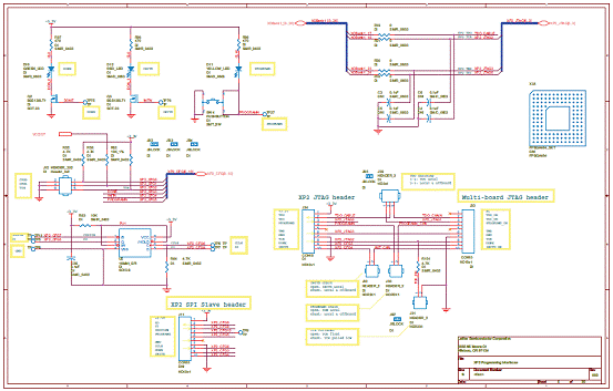
This document (including the schematics in the appendix) describes LatticeXP2 Standard Evaluation Boards marked as Rev 000. This marking can be seen on the etching on the back of the printed circuit board, under the Lattice Semiconductor logo.
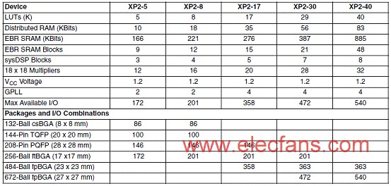
The LatticeXP2 is a third-generation non-volatile FPGA device. It combines a Look-up Table (LUT) based FPGA fabric with Flash Non-volatile cells in a flexiFLASH? architecture. The flexiFLASH approach provides benefits such as instant-on, small footprint, on chip storage with FlashBAK? embedded block memories and Serial TAG memory and design security. The LatticeXP2 also supports live updates with TransFR?, 128-bit AES Encryption and Dual-Boot technologies. The LatticeXP2 devices include LUT-based logic, distributed and embedded memory, Phase Locked Loops (PLLs), pre-engineered source synchronous I/O and enhanced sysDSP? blocks.
图2。LatticeXP2标准评估板外形图
LatticeXP2标准评估板主要特性:
LatticeXP2 Standard Evaluation Board featuring
LatticeXP2-17 FPGA in 484fpBGA package (LFXP2-17E-6F484C)