|
|
一、摘要:
SPI 接口应用十分广泛,在很多情况下,人们会用软件模拟的方法来产生SPI 时序或是采用带SPI 功能模块的MCU。但随着可编程逻辑技术的发展,人们往往需要自己设计简单的SPI 发送模块。本文介绍一种基于FPGA 的将并行数据以SPI 串行方式自动发送出去的方法。
二、关键字:
VHDL、FPGA、SPI、串行数据输出选择模块、移位脉冲产生模块、SPI 时钟采集信号和无相移的SPI 基准时钟产生模块、SPI 时钟输出选择模块、8bit SPI 时钟采集生成模块、16bit SPI 时钟采集生成模块、24bit SPI 时钟采集生成模块、8bit 数据移位模块、16bit 数据移位模块、24bit 数据移位模块。
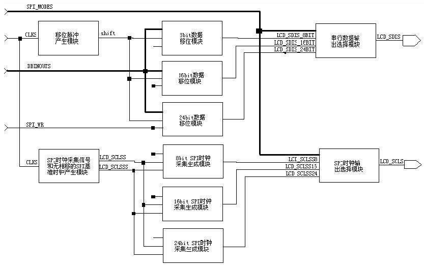
三、功能框图:

SPI_MODES 为输入模式选择端口:
--"01"is 8bit 传输模式
--"10"is 16bit 传输模式
--"11"is 24bit 传输模式
CLKS 为整个模块的基准时钟
DBINOUTS 为并行数据输入端口:
--8bit 模式为DBINOUTS(7 downto 0)
--16bit 模式为DBINOUTS(15 downto 0)
--24bit 模式为DBINOUTS(23 downto 0)
SPI_WR 为启动SPI 传输的信号
整个功能模块可工作在 8bit、16bit、24bit SPI 猝发传输状态。对其进行软件操作的步骤相当简单:
--此模块软件操作流程如下
--1、SPI_MODES="xx" 设定串口操作模式
--2、DBINOUTS="xxxxxxxxxxxxxxxxxxxxxxxx" 输入要发射的数据
--3、SPI_WR='0'
--4、SPI_WR='1'
--5、SPI_WR='0'
--8bit 模式延时2*8*4*CLKS
--16bit 模式延时2*16*4*CLKS
--24bit 模式延时2*24*4*CLKS
--6、DBINOUTS="xxxxxxxxxxxxxxxxxxxxxxxx" 输入下一个要发射的数据
四、VHDL 描述解读
--以下描述的是一个SPI 自动发射模块
--在很多情况下,人们会用软件模拟的方法来产生SPI 时序
--这里采用硬件的方法,即使软件操作更为简单,有提高了传输的速度
--------------------------------------------------------------
--此模块软件操作流程如下
--1、SPI_MODES="xx" 设定串口操作模式
--2、DBINOUTS="xxxxxxxxxxxxxxxxxxxxxxxx" 输入要发射的数据
--3、SPI_WR='0'
--4、SPI_WR='1'
--5、SPI_WR='0'
--8bit 模式延时2*8*4*CLKS
--16bit 模式延时2*16*4*CLKS
--24bit 模式延时2*24*4*CLKS
--6、DBINOUTS="xxxxxxxxxxxxxxxxxxxxxxxx" 输入下一个要发射的数据
library ieee;
use ieee.std_logic_1164.all;
use ieee.std_logic_unsigned.all;
entity SPI_interface is
port(CLKS :in std_logic; --基准时钟
LCD_SCLS :out std_logic;--SPI 发射时钟,上升沿有效
LCD_SDIS :out std_logic;--SPI 数据串行输出口
SPI_MODES :in std_logic_vector(1 downto 0);
--串口操作模式选择
--"01"is 8bit trans mode
--"10"is 16bit trans mode
--"11"is 24bit trans mode
SPI_WR :in std_logic; --启动串口发送信号
DBINOUTS :in std_logic_vector(23 downto 0));
--背发送数据的并行输入口
--8bit mode use DBINOUTS(7 downto 0)
--16bit mode use DBINOUTS(15 downto 0)
--24bit mode use DBINOUTS(23 downto 0)
end;
architecture SPI_interface_behav of SPI_interface is
signal DB8BIT_reg :std_logic_vector(7 downto 0); --8bit 数据移位寄存器
signal DB16BIT_reg :std_logic_vector(15 downto 0);--16bit 数据移位寄存器
signal DB24BIT_reg :std_logic_vector(23 downto 0);--24bit 数据移位寄存器
signal counter4 :std_logic_vector(3 downto 0); --移位脉冲产生计数器
signal counter4s :std_logic_vector(1 downto 0); --SPI 时钟生成计数器
signal counter8 :std_logic_vector(4 downto 0); --8bit SPI 时钟控制计数器
signal counter16 :std_logic_vector(5 downto 0); --16bit SPI 时钟控制计数器
signal counter24 :std_logic_vector(5 downto 0); --24bit SPI 时钟控制计数器
signal shift :std_logic;--移位时钟脉冲
signal LCD_SCLSS :std_logic;--SPI 时钟采集信号
signal LCD_SCLSSS :std_logic;--无相移的SPI 基准时钟
signal LCD_SCLSS8 :std_logic;--8bit SPI 时钟信号
signal LCD_SCLSS16 :std_logic;--16bit SPI 时钟信号
signal LCD_SCLSS24 :std_logic;--24bit SPI 时钟信号
signal LCD_SDIS_8BIT :std_logic;--8bit SPI 数据信号
signal LCD_SDIS_16BIT :std_logic;--16bit SPI 数据信号
signal LCD_SDIS_24BIT :std_logic;--24bit SPI 数据信号
begin
--串行数据输出选择模块
u1:process(LCD_SDIS_8BIT,LCD_SDIS_16BIT,LCD_SDIS_24BIT,SPI_MODES)
begin
if SPI_MODES="01" then --选择8bit 串行数据输出
LCD_SDIS<=LCD_SDIS_8BIT;
elsif SPI_MODES="10" then --选择16bit 串行数据输出
LCD_SDIS<=LCD_SDIS_16BIT;
elsif SPI_MODES="11" then --选择24bit 串行数据输出
LCD_SDIS<=LCD_SDIS_24BIT;
else LCD_SDIS<='1';
end if;
end process;
--移位脉冲产生模块
u2:process(CLKS)
begin
if CLKS='1' and CLKS'event then
if counter4="0011" then
counter4<="0000";
shift <='1';
else counter4<=counter4+1;
shift <='0';
end if;
end if;
end process;
--SPI 时钟采集信号和无相移的SPI 基准时钟产生模块
u3:process(CLKS)
begin
if CLKS='1' and CLKS'event then
if counter4s<"11" then
counter4s<=counter4s+1;
else counter4s<="00";
end if;
end if;
LCD_SCLSS<=counter4s(0); --SPI 时钟采集信号
LCD_SCLSSS<=counter4s(1); --无相移的SPI 基准时钟
end process;
--SPI 时钟输出选择模块
u4:process(LCD_SCLSS8,LCD_SCLSS16,LCD_SCLSS24,SPI_MODES)
begin
if SPI_MODES="01" then
LCD_SCLS<=LCD_SCLSS8; --选择8bit SPI 时钟模式
elsif SPI_MODES="10" then
LCD_SCLS<=LCD_SCLSS16; --选择16bit SPI 时钟模式
elsif SPI_MODES="11" then
LCD_SCLS<=LCD_SCLSS24; --选择24bit SPI 时钟模式
else LCD_SCLS<='1';
end if;
end process;
--8bit SPI 时钟采集生成模块
counter8_u:process(LCD_SCLSS)
begin
if SPI_WR='1' then
counter8<="10001";
elsif LCD_SCLSS='1' and LCD_SCLSS'event then
if counter8>0 then
counter8<=counter8-1;
LCD_SCLSS8<=LCD_SCLSSS;
end if;
end if;
end process;
--16bit SPI 时钟采集生成模块
counter16_u:process(LCD_SCLSS)
begin
if SPI_WR='1' then
counter16<="100001";
elsif LCD_SCLSS='1' and LCD_SCLSS'event then
if counter16>0 then
counter16<=counter16-1;
LCD_SCLSS16<=LCD_SCLSSS;
end if;
end if;
end process;
--24bit SPI 时钟采集生成模块
counter24_u:process(LCD_SCLSS)
begin
if SPI_WR='1' then
counter24<="110011";
elsif LCD_SCLSS='1' and LCD_SCLSS'event then
if counter24>0 then
counter24<=counter24-1;
if (counter24="000000")or(counter24="000001")or
(counter24="110011")or(counter24="000010")then
LCD_SCLSS24<='0';
else
LCD_SCLSS24<=LCD_SCLSSS;
end if;
end if;
end if;
end process;
--8bit 数据移位模块
DB8BIT_U:process(shift,SPI_WR,DBINOUTS)
begin
if SPI_WR='1' then
DB8BIT_reg<=DBINOUTS(7 downto 0);
else
if shift='1' and shift'event then
LCD_SDIS_8BIT<=DB8BIT_reg(0);
DB8BIT_reg(6 downto 0)<=DB8BIT_reg(7 downto 1);
end if;
end if;
end process;
--16bit 数据移位模块
DB16BIT_U:process(shift,SPI_WR,DBINOUTS)
begin
if SPI_WR='1' then
DB16BIT_reg(15 downto 0)<=DBINOUTS(15 downto 0);
else
if shift='1' and shift'event then
LCD_SDIS_16BIT<=DB16BIT_reg(0);
DB16BIT_reg(14 downto 0)<=DB16BIT_reg(15 downto 1);
end if;
end if;
end process;
--24bit 数据移位模块
DB24BIT_U:process(shift,SPI_WR,DBINOUTS)
begin
if SPI_WR='1' then
DB24BIT_reg(23 downto 0)<=DBINOUTS(23 downto 0);
else
if shift='1' and shift'event then
LCD_SDIS_24BIT<=DB24BIT_reg(0);
DB24BIT_reg(22 downto 0)<=DB24BIT_reg(23 downto 1);
end if;
end if;
end process;
end;
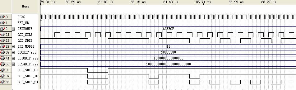
五、仿真波形图
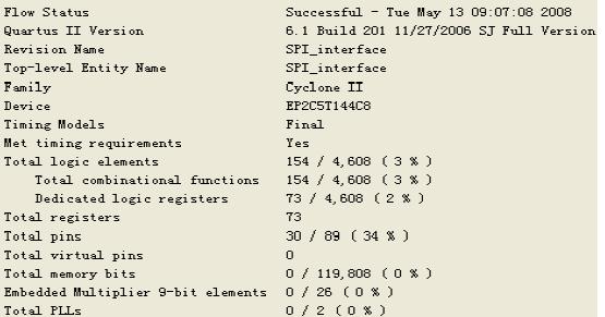
六、编译后资源占用情况
七、结束语
本文旨在给学习可编程技术的人们提供一个参考,起到抛砖引玉的作用。望阅读过此文的读者提供更好的方法,与所有的学习者共享,共勉! |
|


 雷达卡
雷达卡
 发表于 2015-4-27 17:02:19

 QQ好友和群
 QQ空间
QQ空间 腾讯微博
腾讯微博 腾讯朋友
腾讯朋友 微信
微信 收藏
收藏 分享
分享 支持
支持 反对
反对 提升卡
提升卡 置顶卡
置顶卡 沉默卡
沉默卡 喧嚣卡
喧嚣卡 变色卡
变色卡 抢沙发
抢沙发 千斤顶
千斤顶 显身卡
显身卡