| Problem | Cause | Effect |
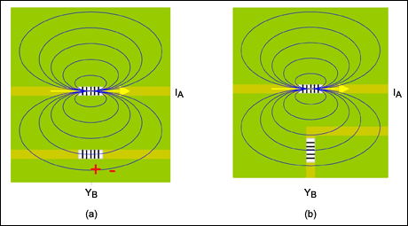
| LNA/tank circuit arrangement (receiver) | Inductor orientation | RF feedthrough |
| Degeneration/π-network arrangement (transmitter) | Inductor orientation | RF feedthrough |
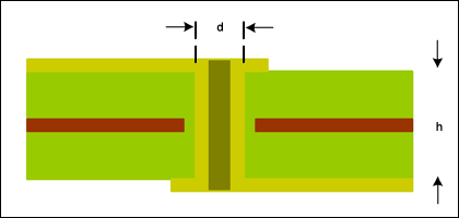
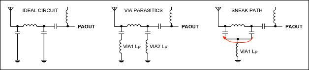
| Shared ground vias between legs of π network | Via parasitics | Feedthrough, RF leakage |
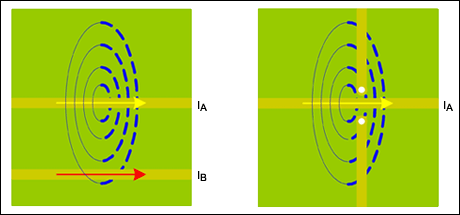
| Shared ground vias between receiver blocks | Via parasitics | Crosstalk, RF feedthrough, RF leakage |
| Long traces for decoupling capacitors | Higher-impedance connections | Reduced decoupling |
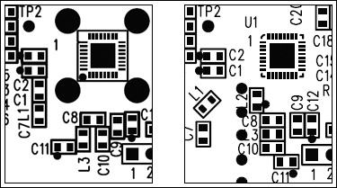
| Wide component placement | Increased parasitics, ground loops | Detuning, crosstalk, feedthrough |
| Colinear traces in the transmitter circuit | Filter bypassing, i.e., power amplifier (PA) directly to antenna | Harmonics radiation |
| Top-layer copper pours | Parasitic coupling | RF leakage, RF interference |
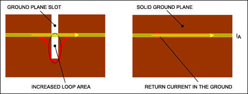
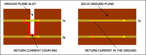
| Discontinuous ground plane | Return current concentration | Crosstalk, feedthrough |
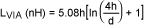
| Crystal connection trace length | Excess capacitance | LO frequency pulling |
| Crystal connection trace separation | Excess capacitance | LO frequency pulling |
| Ground plane under crystal pads | Excess capacitance | LO frequency pulling |
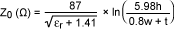
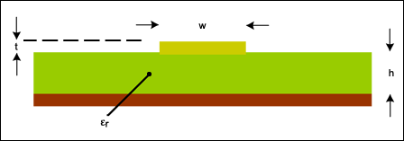
| Planar PCB trace inductors | Poor inductance control | Large footprint, low Q, crosstalk, feedthrough |


 雷达卡
雷达卡
 发表于 2015-4-27 07:06:41


 QQ好友和群
 QQ空间
QQ空间 腾讯微博
腾讯微博 腾讯朋友
腾讯朋友 微信
微信 收藏
收藏 分享
分享 支持
支持 反对
反对 提升卡
提升卡 置顶卡
置顶卡 沉默卡
沉默卡 喧嚣卡
喧嚣卡 变色卡
变色卡 抢沙发
抢沙发 千斤顶
千斤顶 显身卡
显身卡